Layout User Guide
Layout Views and Panels
Display Panel
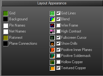 One of the interesting things that PCB123 technical support notices when processing orders is the incredible diversity of color schemes and display settings that different users prefer. Some schemes are quite creative and pleasing to the eye while others seem to offend the senses. The point is that what works for some people, does not always work for others. This becomes especially important on very dense designs or designs that have a complex topology. These designs can lead to the subjective phenomenon of information overload. This can have a negative effect on productivity and can be a major contributor to mental fatigue. Beginners tend to be adversely affected more than experienced users but everyone has a different threshold of overload and fatigue and not everyone agrees on the best way to reduce it. It is for this reason that PCB123 employs a variety of global display settings.
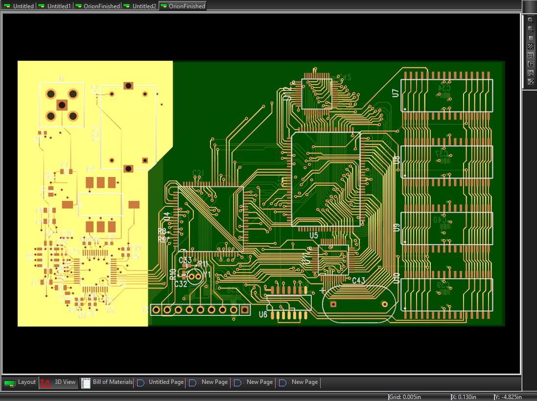
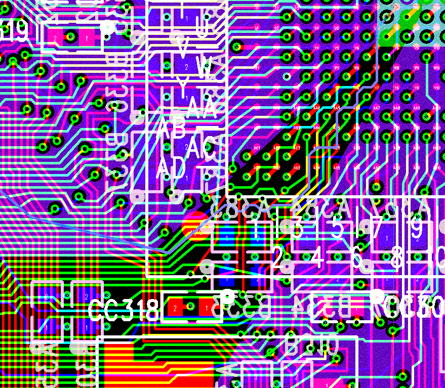 Take a look at the design on the left.
This is a 6-layer design with everything visible, rendered in true width, and with color blending on. Even though the zoom factor is reasonable, the density of objects and the large angular fills make this screen difficult to look at. In this case, there is even confirming evidence of information saturation in that some features have turned white because so many objects with different colors occupy the same screen location.
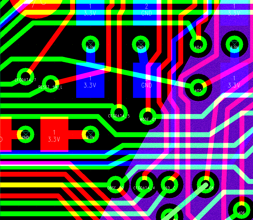 This next picture is with the silkscreen layer set to invisible and the zoom factor has been increased to a greater magnification.
This does not hurt the eyes nearly as much but it is zoomed in so far that it is difficult to move anything without bumping into a window edge.
We will zoom back out to the original scale and try changing the display properties of the objects as opposed to the number of objects displayed.
The first thing we will try is turning off color blend.
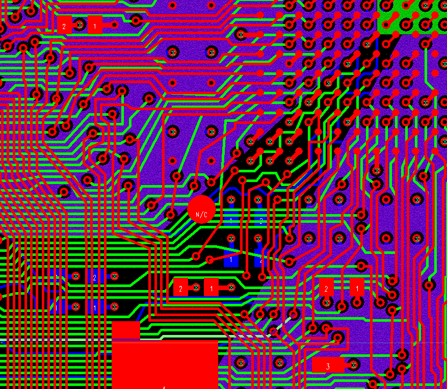
As you can see, the data separation is much better but the opaque copper regions make it impossible to see the layers underneath. If we had to insert a via, we would be shooting blind and would have to keep changing layers to determine if the via would interfere with the obscured layers. Turning color blend off works best when there are no large fill areas.
Next we will try changing the Wireframe setting.
Wireframe does not fill any object interiors. It simply displays either the outline or the center line of an object
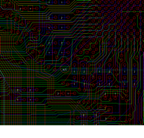
Now this is probably a reasonable screen to look at while finding room to insert a via. It provides visibility to all layers.
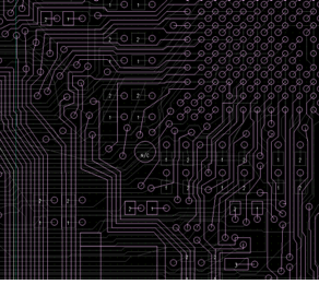
If we had to route an entire trace through the area we might try to use the Hi-Contrast mode in conjunction with Wireframe.
Hi-Contrast always displays the current layer in the contrast color and all other layers are displayed using the same dim color. This mode works great for cycling through layers looking for a path across the window.
Design View
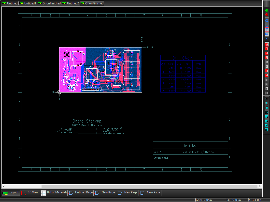
The Design view, also identified as the Layout view is (along with the schematic view) one of the most-accessed views during the board design process.
3D View
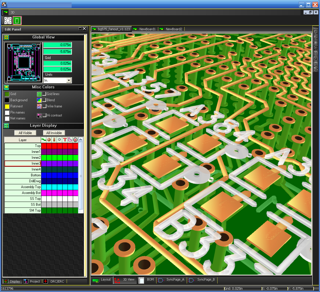
The 3D viewer is a photorealistic rendering system that displays the board in a perspective projection. The board can be viewed from any angle in 3D space.
Footprint Editor
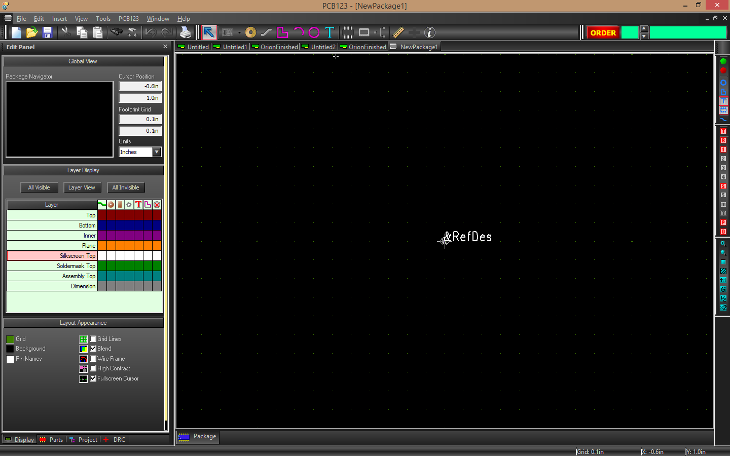
Designing a new footprint requires the use of the footprint editor. The footprint editor can be used as a stacked-interrupt edit function. In other words, as you’re laying out your board, you may discover that the part you wish to use is not yet represented with a footprint in your current libraries. By selecting Design -> New Footprint… you enter the footprint editor window. Note that your layout editor work is maintained in a edit pane underneath the footprint editor.
DRC Panel
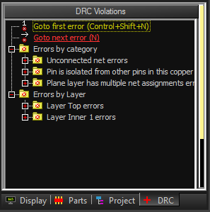
The DRC/ERC tab contains a live listing of all the current design violations in the project.
The DRC will report on shorts, opens, and violations of manufacturing rules such as minimum spacing between objects of different nets, and pad size vs. drill size violations.
Locations of errors reported by the DRC are marked with a grey circle-? icon. By hovering the mouse pointer over the error, users can access a summary explanation for the cause of the error being reported.
The DRC/ERC tab also allows users to access violations by category or by layer. At the top of the DRC/ERC tab are the ‘stepper’ functions, allowing users to move from error to error so as to view/fix each one interactively.
Project Panel
The Project tab contains several report generators and a top-level navigator in the form of a tree that allows you to drill down into the schematic and layout data in minute detail.
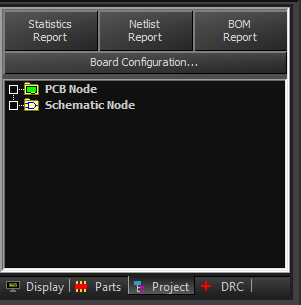
The Statistics Report gives you a summary report on various board metrics for the currently active design, including: board area; routing layers; plane layers; number of components; pins per sq/inch; number of nets; etc.
The Netlist Report generates a netlist to a file location of your choice. You can also opt to view the netlist output in a notepad window.
The BOM Report generates a text file bill of materials in the old-fashioned CAD system part-list format.
The Board Configuration button presents the board configuration wizard dialogs, comparable to the Design -> Board Configuration menu item.
In the nested properties view, near the top of the Project tab, you can navigate down through attributes for virtually every design element in either the schematic or layout side. This includes symbols, footprints, nets, and their individual attributes and identifiers.
PCB Design Tasks
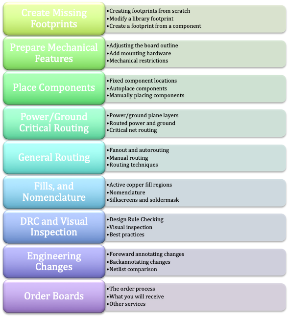
You can view this section as a recipe for creating a PCB. The tasks are listed in roughly chronological order to begin and complete a PCB design. It assumes you are starting the layout from a state listed in Starting a New Design. Some tasks may not apply to your design.
Create missing footprints
PCB123 supplies a library of footprints. Even so, it is inevitable that you will have to create a custom footprint or modify an existing one at some time. Footprints are created or modified in the Footprint Editor, which is very similar to the board editor but does not allow the net or route tools to be invoked.
Additionally, layers are treated generically. There is no concept of a specific layer number, only layer types such as Top, Inner, Plane. In this way, footprints are created board-agnostic. When a footprint is instantiated as a component, features in the footprint are mapped to the physical layers of the board based on the layer type. Some layers do not differentiate between top and bottom such as Silkscreen, Assembly, and Soldermask. This is because any feature placed on these layers will be mapped to the proper layer based on the side of the board any instantiating component is placed. This is a dynamic behavior. As you move the component between top and bottom (by using the Opposite command), the features on the above footprint layers appear on the correct board layers.
Very rarely will you create footprint features on the Plane or Soldermask layers. Any feature created on the Plane or Soldermask layers will result in copper or soldermask being voided, not added to those layers. These layers are traditionally treated as “negative” images. They are a continuous plane of material voided only where objects such as pads have been defined.
PCB123 does not have a traditional padstack object. A pad for a pin is defined simply with a size, shape, and drill. If the drill size is zero then the pad is a surface mount pad and will only appear on the top or bottom routing layer depending on which side of the board the component is placed. If the pin’s drill size is not zero, then the pin is considered a thru-hole pin and a pad will appear on all layers. You are free from the burden of specifying plane layer and soldermask pad features. Plane-layer clearance pads are parametrically derived from the drill size and soldermask clearance pads are parametrically derived from the pad size on the surface routing layer. This not only relieves you of the burden of defining the data but it allows Sunstone to optimize certain processes over time.
Footprints are defined in their own local coordinate system. When a component is placed on a board, its features will be relative to the origin of the footprint. It is recommended that a pin such as pin 1 should be placed at 0, 0 in the footprint. This helps to align component pins during component placement and makes life easier when routing. If you right-click on a pin in the Footprint Editor then one of the context commands is Use Pin as Origin. This will shift everything so that the pin is the new origin.
You can locate a pad at a specific coordinate by invoking the Pin Property dialog. There you can enter the specific X, Y coordinates for the pin using the full power of expressions. This can be quite useful when the mechanical specs locate pins relative to other pins.
If a mechanical drawing is referenced from the bottom view of a part, go ahead, create the footprint in the same way, and then from the main menu select Tools/Mirror All Geometry. This will flip everything back to a topside view, which is how a footprint should be defined.
When you need to create a custom footprint, you can create one from scratch, modify an existing footprint from a library, or create a footprint from a component on a board.
Creating footprints from scratch
With a document open, you can select Design > Create New Footprint from the menu. This will open an untitled Footprint Editor window whose only contents are a reference designator placeholder and the origin marker. When you are finished creating the footprint and you want to save it to a library you will have to name it and choose a library to save it in.
Modify and existing footprint from a library
If you can identify an existing footprint in a library that closely matches the footprint you need then it may be advantageous to start with the close match. Select Design > Edit Footprint and browse the library to select which footprint to edit. This will open a new Footprint Editor Window fully populated with the selected footprint. After making the edits you want, choose the File/Save Footprint As command. This will show the Save Footprint Dialog with all the original information retained such as the footprint name and the library it came from. It is important that you do not overwrite the original footprint; you must choose either another name or a different library to save the modified footprint into. If by accident you overwrite the original, undo all your changes to the footprint and save again. Then you can redo all the changes and save correctly this time.
Use an existing component as a starting point
If you have a component that is close to what you need or you just want to update one or more similar components on a design then you can point at a component in the Design View, right-click, and select Edit Footprint from the context menu. This will open a new Footprint Editor Window fully populated from the contents of the component. If, after making all changes, you want to save the footprint to a library then choose the File/Save Footprint As command. Whether you save the footprint to a library or not, closing the window will prompt you with the Update Components Dialog, which lets you decide how you want to apply the changes to the design that you started the edits with.
Prepare Mechanical Features
PCB123 supports the ability to import common mechanical CAD file formats for use as the board outline. Find the options to import IDF or DXF data on the PCB123 main menu listing.
Adjusting the board outline
When you first create a new design, you acquire a board outline in one of five ways:
use the default board outline in which case you have a 5” x 3” rectangle,
specify some other rectangle,
load a board template that already has a board outline,
use a gutted previous design for the board outline.
Import and IDF outline from your mechanical CAD tools via the
PCB123 -> IDF Import/Export plugin.
In any event, you may need to adjust the board outline manually.
To move an entire board outline just left click on it and hold then drag, releasing the mouse button when you have positioned the board outline where you want.
Moving a board outline corner is simple: just point at a board outline corner, left-click, and release. Now you are moving a board outline corner. Just click again to release the corner where you want.
Mouse over a corner and press the d key to delete a corner of the board outline or any other polygon shape. Deleting a corner can also be accomplished with the mouse simply by selecting a corner and dropping it on the previous or next corner in the board outline. It is called corner reduction. It is very efficient, and can all be done with the mouse.
To insert a corner in a board outline simply click on the middle third of a segment or at least .050” away from a corner. You will then be in digitizing mode that allows you to add corners until you stop by pressing the Esc key, double clicking, or inserting another corner at the same location as the previous one.
Add mounting hardware
Mounting hardware can be in many forms, but usually it will use a drilled hole. Depending upon your specific needs, these holes can be either plated (PTH) or non-plated (NPTH).
The Maximum hole size available through the pcb123 service using the Add Pin tool is 0.257” diameter. If you require a hole larger than 0.257”, you can use the new Create Cutout tool  . You can then select to either draw a circular or rectangular cutout.

To add a NPTH to your board, click on the add pin icon  . The pin properties form will appear at the top of the Edit Panel. Enter the pin name, click on Non-Plated, and select a size that will be appropriate for your application. Put the NPTH in the desired location.
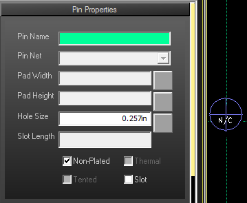 To select, change, or move the hole after it is placed, you will need to make the ‘DrillDwg’ layer visible.
Right mouse click over the NPTH and click on properties.
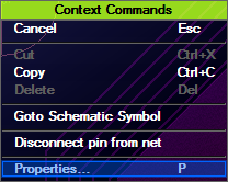
Enter the change that you require in the form that pops up. The only options you will have are size and location. This is where you can fine-tune the placement without changing your grid.
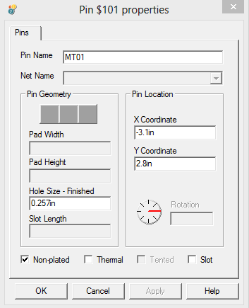
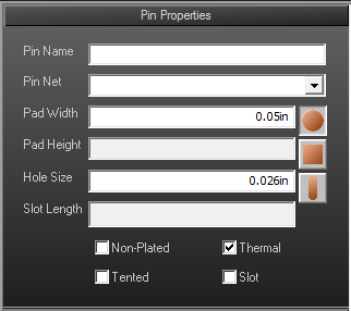
Plated through holes (PTH) can be manipulated in much the same way, but they will have more features for you to define.
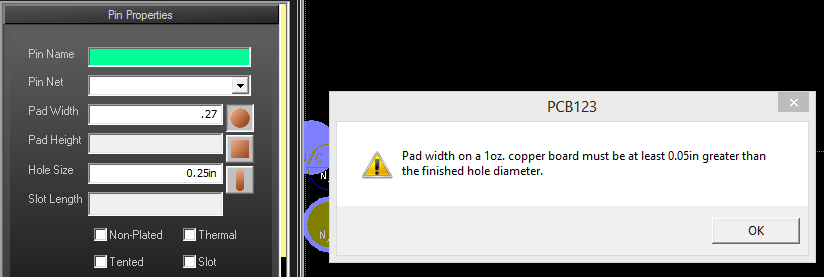
The PTH size will be offered with a default pad width. While you can make the pad size larger than the default, you will not be able to enter a size smaller than the default. Pad width should be large enough to provide a full width contact for any mounting hardware used. Be sure to use the maximum dimension shown on your hardware datasheet for this feature.
The Tented check box sets the solder mask property for a pin. Checking the tented box will cover (Tent) a through-hole pin or surface mount pad. Un-checking this option (the default setting) will create an opening in the solder mask for a through-hole pin or surface mount pad.
The Thermal check box determines if a through-hole pin or surface mount pad will connect to a filled copper region or plane layer with a thermal relief. Selecting the thermal check box will create a connection to polygon or plane with a thermal relief. Un-checking this box will allow a pin to directly connect to the polygon or plane.

The Slot check box is new to PCB123 v5. Checking this option will allow you to create plated an non-plated slots in your layout. Checking the Slot box enables the Slot Length field. Selecting a square or oval pad shape enables the Pad Height field. Set you slot properties and place the object.
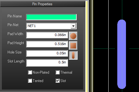
Another new feature in V5 is the removal of the list of pre-defined finished hole sizes. In prior releases you were limited to a set of finished holes sizes. You can now enter in a specific hole size and we will build as designed. The smallest plated hole you can enter is .008” and the largest is .025”. The smallest non-plated hole is .0135” and the largest is .257”.
You can also set a specific hole size for slots. The smallest plated slot hole size is .025” and the largest is .25”. The smallest non-plated slot hole size is .031” and the largest is .257”.
Place components
If you did not start with a netlist then you are probably inserting components manually and placing them roughly where you think they should go as best you can without the aid of a netlist.
If you did start with a netlist then all the components are spread out beneath the board outline showing the ratsnest of connections to be routed.
Fixed component locations
The most logical way to begin placing the board is to identify all the components with fixed locations and place them first. You can right-click on a component to display its properties and from there enter the precise location for that component. Even if the locations are not precisely fixed starting you placement with the I/O circuitry is usually a smart strategy.
Before you start placing the bulk of the components, you should select a reasonable placement grid for the components. The larger the grid the easier it is to align and uniformly distribute components. On very dense boards, it may become impossible to place every device on the same grid. Having the bulk of the pins on a uniform grid can pay big dividends while routing.
After placing fixed, I/O, or generally critical components there are a couple of strategies to employ for placing the remainder of the components:
If you have the schematic handy then you can press Ctrl+F to find and select other components and snap them to the cursor for placement.
If you started with a netlist, you can also use the resulting ratsnest as a placement guide. By roughly placing the devices with the larger pin counts, you try to minimize the overall connection length by placing components that heavily interconnected close together.
These are just some rough guidelines. You design may have some restrictions such as critical nets that dictate a less-than-optimal placement for overall routing, or there may be height restrictions on some devices.
Autoplace components
To get a quick start on the layout process, you may choose to use the menu item, Design -> AutoPlace. Using this function, PCB123 will make its best effort to pre-arrange component footprints in a way to minimize the amount of routing required.
Smart Auto-placement is a complex algorithm that often relies heavily on heuristics and ‘best practices.’ The Auto-Place function in PCB123, while useful, is not intended to be a full-blown autoplacer in the spirit of some other enterprise-level tools.
PCB123 provides an Autoplace function as well. While you create the schematic for your design, PCB123 tracks both the schematic symbol in the schematic sheet, and the associated footprint for that schematic symbol. As you place symbols, the footprints and rats-nest connection data are queuing up on the layout view, ready for placement and routing.
Auto placement is a good tool for getting all of the component footprints on the screen. After that, they will all probably still need to be moved into a more appropriate location. The auto-placement feature has no practical idea what each component’s relation to the other components on the board might be. For example, if your decoupling capacitors are all lined up on page three of your schematic, with ICs on page 1 and 2, your decoupling capacitors will all place in a little patch of real estate independent of any relationship they may have in the real world.
The autoplacer can be used iteratively as you work through the initial placements on your board. Use the LOCK setting on the component properties pane to lock down a component and keep the autoplacer from relocating it.
Manual place components
Pragmatically speaking, whether you’ve used AutoPlace or not, you’ll probably want to do some amount of manual placement of components.
If the component footprints are already placed on your layout view, you can manually adjust the component placement. Click on the  selection tool. In selection mode, hover the mouse pointer over a component until the mouse cursor turns into a chip package icon. Then left-click the component to enter move mode. The component will ghost interactively on the screen; place the component in its new location. Ratsnest data will follow; previously routed connections will ratsnest from any broken connections to the component in its new location.
Power, ground, and critical routing
Power and ground plane layers
In this section, we’ll show you how to add a Plane to the routing layer, and name the plane ‘+12v’
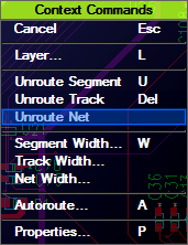
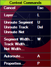
In this case we have selected a trace on the +12V net. Clicking on the Unroute Net menu item will remove+12V trace routing from all layers
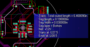
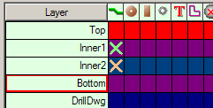
Set the edit layer to layer Bottom, using the edit pane on the left side of PCB123.
Click on the add Draw Polygon icon, draw a polygon around the board to cover the area under all +12V pins from any layer. It helps to check bottom layer routing and adjust any traces that will cut across the plane. 
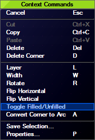
The plane you draw will be just an outline with default line width. Right mouse over the new polygon you drew and select Toggle Filled/Unfilled.
This is your filled polygon. It is named 12VPLANE, but not attached to a net yet.
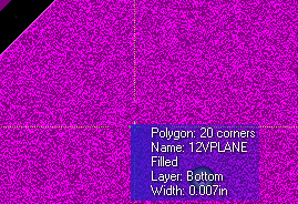
Right mouse over the plane area again, select the net name (+12V) and ok the form.
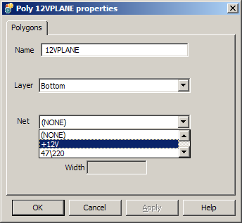
Now, Route all +12V pins out to a breakout via to finish your connections.
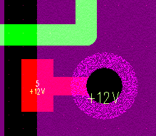
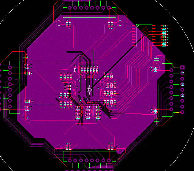
Reroute your pre-existing traces, and cleanup.
If your board has a large number of power and ground pins, if it will be drawing a high current, or if there are high speed signals, you will want to add plane layers to your board.
Sometimes you will need both power and ground, others just ground layers will be sufficient, with routed power.
To define an internal layer as a power or ground layer has been simplified as compared to many other cad programs you may have seen:
Open your pcb123 layout window.
Click on Design, Board Configuration.
Select Four or Six layer Board, this will also free up the ‘Use Inner as plane layer buttons.
Select the layers you want to make into plane layers.

Or,

Click the Ok button.
Typically you will want to alternate signal and plane layers, keeping each signal layer adjacent to a plane layer. The pictures above show a typical setup for a 4 or 6 layer board.
Place your cursor over a ratsnest/guide for your power or ground net to be assigned a plane layer, press the right mouse button, select properties.
In the Net xxx properties menu, (my net is called “sink”) select the plane or planes that will connect to your net.
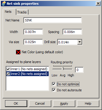
The only thing left to make your power/ground connections will be routing from surface mount pins to a via for connectivity.
For power or ground that will be attached to a plane layer, I would not want to auto-route the net, since doing so would add a huge amount of clutter to the signal routing layers. You may want to use the auto-router to perform breakout, but after that, turn off auto-routing for your power/ground nets.
Routed power and ground
As your boards become more complex, you will have more than just one or two power nets.
When this happens, you may need to manually route some of them.
You will still not want to auto-route power or ground due to the amount of clutter that this can create.
Power should be routed before your other circuitry in order to ensure that you leave enough room to get the job done. Power traces are typically wider than signal traces, and usually need extra spacing to keep from negatively affecting your more sensitive signals.
Power and ground nets usually make use of discrete components such as caps, resistors, inductors, etc… These parts can have specific placement and routing constraints that will not be possible if you have already routed the rest of your nets.
Some things that need to be taken into account before you start routing your power are;
Current present on the net. (how wide do the traces need to be?)
Voltage, difference between the net and other nets on the board. (how far apart do your nets need to be for safety reasons)
Space required from sensitive nets, amount of ‘noise’ on the net will have to be considered. (do some nets need to be farther from your power nets to work?)
Decoupling, bypass, and bulk capacitors will need to be carefully placed and routed prior to power net routing.
Make a plan, it’s sometimes best to do it on paper with colored pens to make sure you can make your connections before spending a bunch of time in cad just to find out that you need to rip everything up and spread your parts out for more room.
Critical routing
Some nets may have special needs such as a minimal routing length or routed in a particular sequence from pin to pin. Often it is easier to deal with these nets at the beginning then later on in the design when things may get dense.
Clock nets should be routed first and very carefully planned out. These nets control pretty much everything else that happens on your board, and if clocks are not properly connected and protected, nothing else will really work as well as you hope.
Any nets with a specific timing requirement should be routed next. Nets such as usb, data and address lines, etc… should be carefully scrutinized for length, spacing, and impedance requirements prior to making the actual connections on your board.
Some nets will require “differential pair” routing, two nets running carefully side by side for the entire distance that they travel across your board.
Once routed, these “critical routing” traces should be left alone and only moved if there is no other option.
General routing
General nets are any nets that don’t have special routing or other requirements.
All you really need to do is connect them from one pin to another.
These nets will be hooked up after all of your power, ground, and critical nets are complete.
You will still want to make use of a neat and tidy routing plan for these non-critical nets or you will quickly run out of room. While the temptation to auto-route them is always present, your board will look better and almost always perform better if you manually route them.
Routing should follow some rules in order to make the most efficient use of the board area you have;
Route orthogonally where possible. Each layer is set up to route one direction, either horizontally or vertically.
Use 45” chamfered corners when routing. This makes for shorter overall routing, fewer roadblocks, and will reduce unwanted reflections on your signals.
Route straight out of component pins a distance equal to the width of the trace before changing direction. This will remove acute angle features resulting in ‘acid traps’ at board fabrication. Acid traps are sharp corners that can be hard to clean during etching processes. They can result in long term reliability problems on your finished product.
Don’t run these types of traces right next to your critical routing nets, they can cause crosstalk or timing problems on your critical nets.
Fanout and autorouting
If your board has a considerable percentage of surface-mounted devices then you may want to perform a Fanout on your design, especially if your board is dense or has more than two routing layers. The idea behind this is that you have to route out of the SMD pads on the layer they are on so you may as well make sure you can at least escape the pad to an immediate via. Once this is done, you have the option of routing the remainder of the connection on any suitable layer. Besides automatically fanning out a board you can do it manually by routing out of a pad and then pressing the ‘V’ key to terminate the route at a via. You can always remove unneeded vias after the board is complete.
On dense boards, running the autorouter can be beneficial in determining trouble spots on the board. The autorouter settings can be modified in the User Preferences Dialog. You can always undo the results of an autoroute. Autorouting may be an acceptable solution on sparsely to moderately dense designs or designs that have very good connection ‘flow’ to them.
Using the automatic fanout feature can radically decrease the amount of time spent just breaking out your signals from surface mount components.
The automatic fanout tool is preset to use your routing grid for via placement. It will place vias in locations that may not be perfect for your application. On one test (shown below) components were placed top and bottom of the board. Via fanout was run and vias were placed in locations that short two nets together. These vias or components will need to be moved prior to any other routing activity.
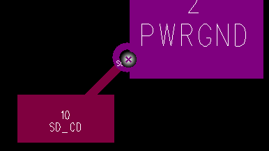
Via placement shown below resulting from automatic via fanout. The vias on sd_wp net are not necessary, traces should be routed directly from pin to pin for this net. Vias can easily be removed from these locations.

After running automatic fanout, and before running the autorouter, you will want to clean up any undesirable fanout vias, perform any power net, and critical routing, make sure your routing grid is set to a number that makes sense for your circuit, turn off fanout before autorouting, setup layer bias and direction, and hit the go button.
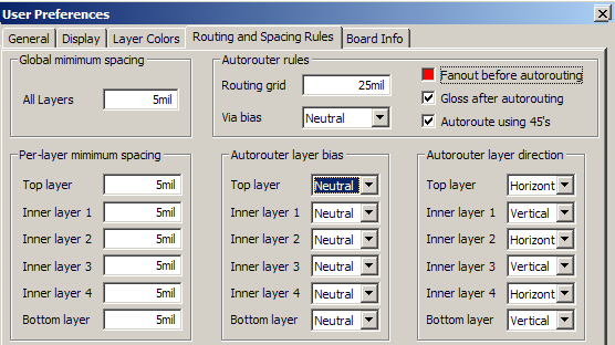
It makes sense to limit the number of layers that you use for autorouting. Doing so will limit the number of layer transitions that your signals make before they reach their destination. You can also limit the number of vias using the via bias option. The options are Use freely, neutral, avoid using, and no vias. Just remember, less is better in most cases.
After your autorouting run is complete, you should do some cleanup. One of the things that needs to be done is management of your signal return path.
Signal return path is the route that your signal will find along the path of lowest impedance, hopefully directly under the actual signal trace as routed on the board.
To help visualize this, think of your house wiring. There is a black wire and a white wire. (we won’t worry about the safety ground, bare wire right now).
The black wire can be considered the signal wire. The white wire provides the signal return. They are spaced very carefully in their cable assembly to provide a controlled and reasonably low impedance signal return. If you simply ran a wire from the breaker out to all of the appliances on the net, and looped it back to the breaker box ground rail, the lights would come on but the tv and radio would suffer from uncontrolled static. On your circuit board this is called ‘noise’. It can usually be controlled by taking a few fairly simple steps that I will try to describe for you.
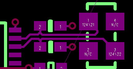
For the circuit below, we have outer signal layers, and inner plane layers. The plane layers are named PWRGND and +3.3V in this area of the board.
Net 124/19 is routed such that it requires a via to transition from top to bottom layer at pin 1 of the pullup resistor shown. In order to provide a good signal return path, you would place a bypass capacitor as shown with a via to each of the reference planes. This will be necessary each location that the net changes from top to bottom layer.
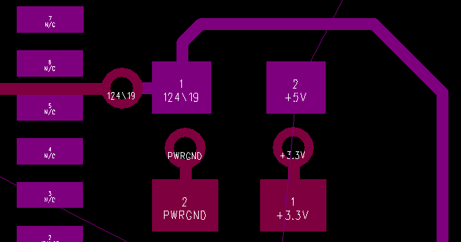
For places where the routing layer changes and there are two ground layers, using a via to tie the ground layers together near your signal via will provide the same service as the bypass capacitor between PWRGND and +3.3V shown above.
Depending on the signal rise time, power, and timing requirements, along with a huge array of other considerations, one bypass capacitor/ return via may suffice for a number of signals in an area, or you may want one to one coverage.
Manual routing
Using the Freestyle tool you can freely insert routes from pins and other routes. You can even define new connectivity this way. There is no auto-finish because there is no end-point defined. The route is terminated by pressing the escape key (leaving a dangling end) or by routing to another pin or route.
In order to make the most efficient use of real estate on your boards, you can manually route all of the signals. This is the preferred method for boards that will be visible to the end user for a lot of reasons. Manually placed and routed boards, when done carefully, just look better than the most carefully autorouted boards. Manually routed boards will also have less vias, can require less layers, and will usually perform better in the field.
In order to manually route your signals, you will want to make sure that you follow the order of routing precedence described above. Route your power according to specific current and voltage rules to provide a safe and robust power delivery system.
Route clocks and other high speed nets to meet the requirements outlined in their specifications.
Connect all of your other general routing nets to complete your board.
Below is a crystal routed with it’s decoupling capacitors. Routing should be as short as possible, nets should be routed together as a differential pair, and the wire length should be matched as closely as practical. Again, this should not be a problem because you can make any adjustments now, before other routing clutters up your board.
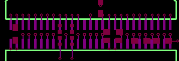
The automatic fanout of the pins on these memory chips will result in very crowded trace routing, and area fill splits between the vias. Moving the vias to a staggered pattern will relieve these problem areas.
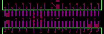
Something like this will provide much more routing space for the signals running between these memory parts.
Routing techniques
Routing should be orthogonal with mitered corners in order to make efficient use of your board area.
Routing with random angle traces will be very hard to maintain and will take much more space since traces can’t be routed parallel to each other.
Mitered corners are important for reduction of signal reflection which causes noise and timing problems. Mitered corners also reduce the amount of area that your traces use on the board
When manually routing a net connecting two pins that are not located on your routing grid; start routing from one pin, route most of the trace but stop before you make the last connection, hit the esc. Button on your keyboard to stop routing, move your cursor to the unrouted pin, click on it to start routing, finish routing the wire to provide neat pad entry and on-grid trace routing.
Fills, and Nomenclature
Active copper fill regions
In order to have more than one power or ground net represented on a single layer, you will frequently add a copper fill for each of your power/ground nets.
To reduce the likelihood of errors in your connectivity, you will need to attach each power fill region to a specific net name.
In the example below, we will add a power plane to +12V.
If the net is already routed, you will want to unroute all of the traces on that net.
Center mouse over trace on net to be removed. In this case we have selected a trace on the +12V net. Clicking on the Unroute Net menu item will remove+12V trace routing from all layers.


You will have ratsnest guides showing for the power net now, making it more obvious where all of the connections need to be made.
Set your edit layer to your intended power or ground layer In this case, it will be layer ‘Bottom’.

Click on the add Polygon icon, draw a polygon around the board to cover the area under all +12V pins from any layer. It helps to check bottom layer routing and adjust any traces that will cut across the plane.
The poly properties menu will open above the display window, simply enter the information that you need to define your plane and start drawing it on the board.
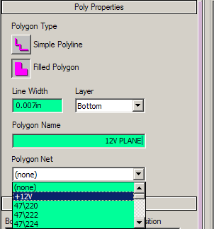
Your area fill will attach to any items that are connected to +12V and pass through or reside on layer ‘bottom’.
Route all +12V pins out to a breakout via to finish your connections.

Gerber output will automatically be generated with thermal relief patterns for all pins and vias.
Nomenclature
Nomenclature, or silkscreen is printed on your board using a non-conductive epoxy, usually in a contrasting color from silkscreen layers. If your board will have visible nomenclature such as reference designators, part number, revision, etc… you will need to adjust it’s placement and sometimes it’s size.
Text size needs to be large enough for us to print legibly, but not so large that it can’t be placed neatly on your board.
A reasonable size for nomenclature is 0.050” tall characters, 0.006” – 0.008” line width.
0.006” is the minimum line width that we can print with a guarantee that it will be complete and legible.
To edit information text such as company information or board part number, click on the add text button at the top of your edit window.

Enter your required text using the keyboard, or you can copy and paste from another document for quicker more accurate entry.
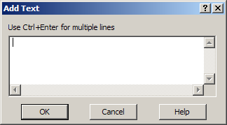
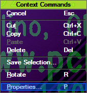
To edit text size, orientation, line width, layer, etc… after text entry, right mouse click on Properties,
Make any changes to the form that you feel would improve the look and legibility of your text items and click on ok..
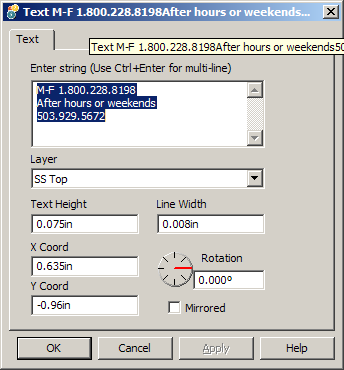
The same changes can be done to component name, reference designators shown in the popup menu below.
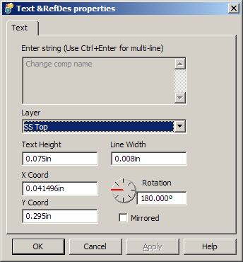
After your text has the size and thickness that you like to see, you may have to move it to a more likely location.
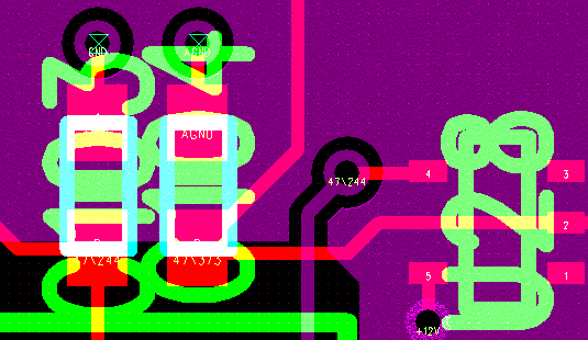
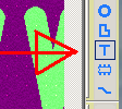
Set your select filter to text using the icon shown below.
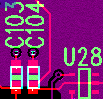
Put your cursor over a text item that needs to move, right mouse to select and simply drag the text to it’s new location
While the text is selected, push the letter R (upper or lower case is fine) and the text will rotate 90degrees (U28 had to be rotated 270 degrees so “RRR” did the trick.
Order Boards
PCB123 is unique in that the tool tracks your design against a fully documented set of manufacturing process parameters. In fact, because of the close connection between the tool and manufacturing capabilities at Sunstone Circuits, PCB123 can even provide real-time quoting for board fabrication as you design.
The in-tool quote-and-order functionality provides you with two key benefits:
You can design to your fabrication budget, and get immediate notification if a design change affects your pricing.
Thanks to the web interface ordering process, you can efficiently submit your design to Sunstone for manufacture, with a clear understanding of the manufacturability (thanks to DRCs) and pricing for your order.
The order process itself is quite easy On the following pages, we’ll walk you through the ordering process.
The Order process
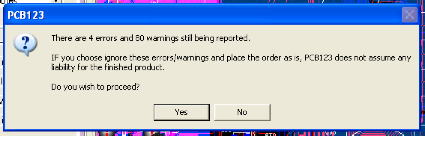
Pre-Order DRC check
Sunstone Account Log-in
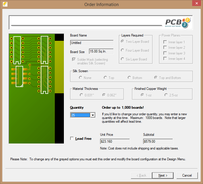
Board Configuration Review Page. You can review the settings used for the board being ordered. On this page, at this point in the process, you can modify the board quantity, and the ROHS manufacturing options. Any other configuration options will require quitting the order process and accessing the board configuration inside the editor environment.
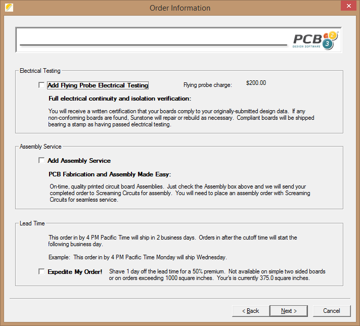
Add On Services Page. Additional services can be selected here. As of this printing, PCB123 provides the following cost-adder services:
- Flying Probe Electrical Testing
- Assembly services (via a partner company)
- Expedited manufacturing
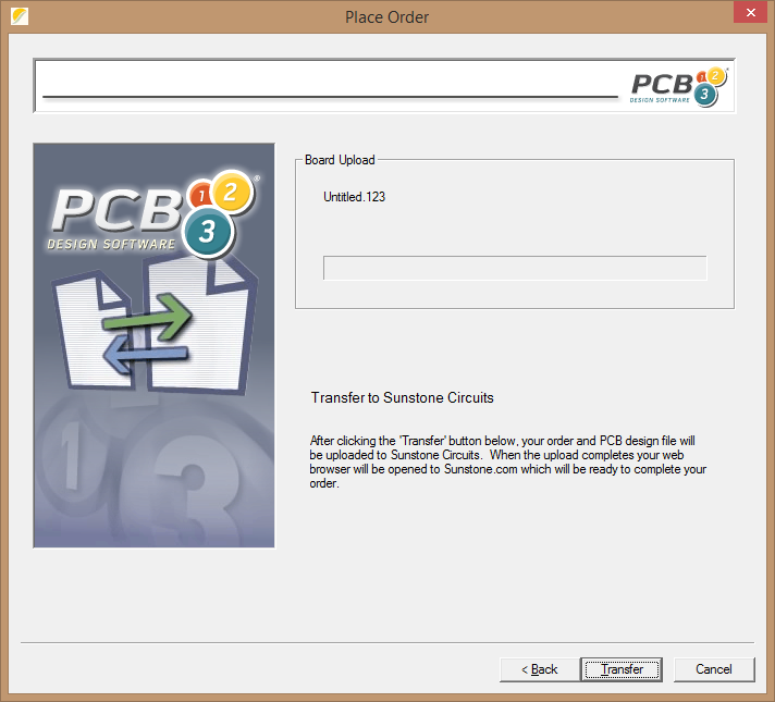
File Transfer. Click the transfer button on this page, and your PCB123 design file will be transferred via your internet connection to Sunstone Circuits. Along with the design file we will receive the board configuration and basic manufacturing parameters you specified in step 2. Please note, your order is not yet complete. But, the only remaining steps are the payment details.
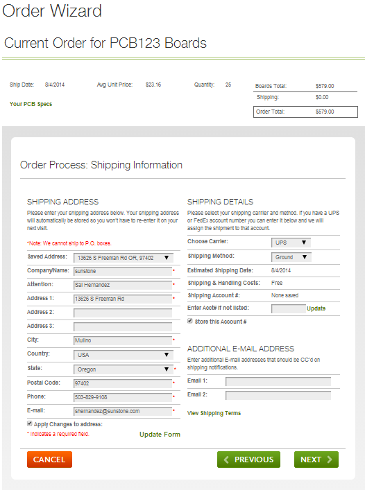
Shipping Information. After the transfer is complete, order control transfers to a web browser page similar to the example below. Enter your shipping details, ship method, ship account number and select Next to continue.
Payment Information. Here you can either enter credit card or billing information or, if you have credit card information already on file in your Sunstone account, you can choose the pre-loaded information. This page confirms the cost-adder services you may have selected, and also shows you the estimated ship date. Please be aware that, for some payment options like Phone/FAX, your order will not be released to manufacturing until payment information is received by Sunstone Circuits. As such, the ship date is an estimate until payment is confirmed.
Click next on this page, and you proceed to order confirmation
Review and Submit Order: Final confirmation of the order, services, ship date, options, etc. At this point, all payment and manufacturing information is complete. Clicking the SUBMIT ORDER button places the order and initiates the process to charge the credit card account.
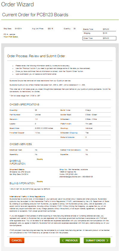
And that completes the order process. Your order appears in the PCB123 order queue at Sunstone Circuits and immediately moves onto the manufacturing floor for tooling, imaging and manufacture.
You can check on the status of your order (including where it is in manufacturing) at any time by logging into your account at www.sunstone.com.
Routing your Design
Before you route
After you have all the components placed on the board, you may need to setup special rules for some nets. These include:
Plane Layer Nets: If you have plane layers, you will need to establish which nets are tied to the planes. You can navigate to the nets in the Object Hierarchy or graphically select the nets and use RMB Properties to get to the Net Properties Dialog. Assuming you have already identified at least one inner layer as a plane layer you can click on the plane layer checkboxes in the net properties dialog. This tells the system that as soon as a pin connects to a plane layer either because it is a thru-hole pin, it is routed to another thru-hole pin or via, then it is considered connected. If you have multiple nets assigned to the same plane layer you will have to isolate the pins from each net by adding a polyline that encompasses just the pins of one of the plane nets. This has to be done manually.
Special Net Widths: Depending on the copper weight of the board, the default width of nets will be either .007” or .012”. This may not be adequate for certain nets, especially those that may be carrying higher current. You can set the line width for these nets in Net Properties Dialog.
Special Net Spacing: Depending on the copper weight of the board, the default spacing for nets will be either .007” or .012”. This may not be adequate for certain nets, especially those that may be carrying a high potential and need to meet regulatory requirements or nets that are edge sensitive and need to ensure minimal coupling. You can set the net spacing in the Net Properties Dialog.
You can also set Per-Layer spacing rules in the User Preferences Dialog.
Routing the board
After you have all the components placed on the board, your next task is to route all the nets. There are many factors to consider and there are many tools to help. Generally, you want each layer to have a preferred routing direction or ‘flow’. Too much meandering on a layer most likely will cut off routing channels before all the routing is complete.
As for a routing strategy, here is a sequence to consider:
Fanout: If your board has a considerable percentage of surface-mounted devices then you may want to perform a Fanout on your design, especially if your board is dense or has more than two routing layers. The idea behind this is that you have to route out of the SMD pads on the layer they are on so you may as well make sure you can at least escape the pad to an immediate via. Once this is done, you have the option of routing the remainder of the connection on any suitable layer. Besides automatically fanning out a board you can do it manually by routing out of a pad and then pressing the ‘V’ key to terminate the route at a via. You can always remove unneeded vias after the board is complete.
Critical Routing: Some nets may have special needs such as a minimal routing length or routed in a particular sequence from pin to pin. Often it is easier to deal with these nets at the beginning then later on in the design when things may get dense.
Short connections: Short connections are very easy to route at the start of a design but because of limited options can be extremely difficult to route on a dense board if saved until the end.
Wide Traces: for the same reasons as mentioned above.
For general routing, you have several options available to you:
Autoroute: This may be an acceptable solution on sparse to moderately dense designs or designs that have very good connection ‘flow’ to them. On dense boards, running the autorouter can be beneficial in determining trouble spots on the board. The autorouter settings can be modified in the User Preferences Dialog. You can always undo the results of an autoroute.
Partial Autoroute: You can select a connection or group of connections, right-click the mouse, and select Autoroute from the context menu. This will engage the autorouter for just those connections.
Pin-To-Pin Manual Routing: If you started your design with a netlist then you can just click on a connection (ratline) and start digitizing corners. Because there is knowledge of where the connection terminates you can double click at anytime and the system will automatically finish routing the connection using a straight line or an orthogonal pair of lines. This type of auto-finish does not avoid obstacles and may produce DRC markers.
Freestyle Manual Routing: Using the Freestyle tool you can freely insert routes from pins and other routes. You can even define new connectivity this way. There is no auto-finish because there is no end-point defined. The route is terminated by pressing the escape key (leaving a dangling end) or by routing to another pin or route.
For manual routing, there are two broad strategies. One of them is intuitive and the other is less intuitive but can be a very powerful technique on dense designs.
Complete each Connection, one at a time: this is an obvious technique that involves selecting or inserting connections, one at a time, and then routing them to completion. It may require a lot of panning around and can possibly lead to a large amount of rerouting toward the end of dense designs.
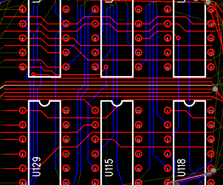
Sweep route one window at a time: take a look at the picture below. It shows one completely routed window of a design. The idea is to zoom in to a comfortable magnification and to route everything in that window. If a connection passes through the window on a diagonal, then drag it to a corner and ‘tack’ it there because it has no business in the current window. If you did not turn off angle snap in User Preferences then you may have to override the snap behavior by holding down the Ctrl key while routing. For connections that pass orthogonally through the window use the same tactic but find an open channel in the window and route it through the window. Once the window is complete, pan to the next window and route that one. You should start in the densest region of the board and pan against the long axis of the board, I.E. if the board is mostly horizontal then pan vertically as your primary pan direction. This very powerful technique results in less rerouting and can identify serious trouble quicker than any other method.
Adding copper regions
If you need to add shielding around nets or generally make other nets as wide as possible a simple method to do this is to add copper pour regions to your design. Simply draw a closed board outline that has been assigned to a net. Objects that are contained within the board outline region that do not belong to the board outline’s net will be isolated from the copper region. Those that are assigned to the same net will be tied to the copper region.
In the picture below, NET1 is surrounded by a copper pour that has been assigned to the GND net. Copper pour does not flood over anything that has a different net property than itself. Even pins that do have the same net property as the copper are cleared out and tied to the copper through ‘spokes’ to help soldering by focusing the heat on the pin.
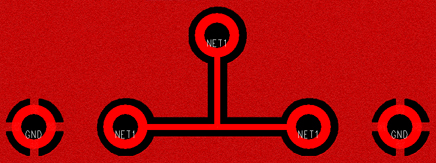
The default isolation gap between copper pour and other objects is 0.008” for standard 1oz copper clad and 0.013” for 2.5oz copper clad boards. This clearance may be increased on certain objects whose net spacing rule dictate a greater clearance, including the copper pour net itself. By specifying worst case spacing on grounds and voltages, copper pour can be safely used while guaranteeing adherence to standards and regulation bodies requirements such as Underwriter Labs (UL).
Care must be taken when adding copper pour to congested areas so that pins are not isolated. Pins that belong to the same net have connection lines, or a ratsnest between them. The connection lines disappear when:
A continuous routed path is completed between the pins.
The pins’ net is assigned to a plane layer and the pins hit the plane layer through a plated hole.
The pins are contained in a copper pour region assigned to the same net.
Because the display of the ratsnest is calculated on the fly, connections made with copper pour are assumed to be complete. However, this may not always be true. It is possible to isolate pins by carving up the copper pour region with too many other-net objects.
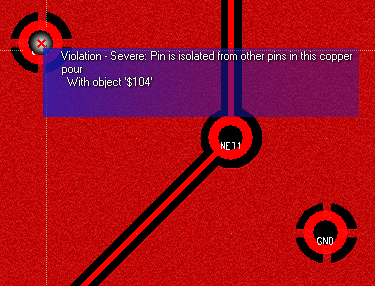
Running a full DRC check on the board will detect possible isolations and the resulting error markers should be investigated carefully. The DRC check for isolations is pessimistic. First, It rasterizes the copper region at some minimum feature size so a pin might be flagged as isolated even though it may be connected by one or more slivers smaller than 0.004”. Second, the isolation check is performed on a per-copper pour basis without regard to the rest of the net topology. This means that two pins inside a copper pour region of the same net may be reported as isolated even though they are connected by a different means such as another copper pour region on a different layer or even a plane layer. This may be corrected in the future but is currently considered beyond the scope of the software.
An example of isolated pins and the corresponding DRC error marker is shown to the left. Note that only one pin is reported as isolated as the other is considered connected to the copper. Only the smallest number of isolated pins is reported by the DRC. The largest connected set of pins is not reported as isolated to reduce the number of error markers generated.
You can also add solid regions of copper that do not clear anything out by simply leaving the net property blank.
If you add a board outline to a plane layer or a soldermask layer, you are actually clearing copper or soldermask from that region because those layers are assumed to be continuous planes and anything on them is considered a break in the plane.
Design Changes
Design changes are an inevitable unpleasant fact so PCB123 has provided some tools to make incorporating design changes as simple and painless as possible. There are two methods for performing design changes. They are:
Manual Changes: some types of changes are obvious. Adding a new component is as simple as clicking on the Add Component toolbar button and adding a connection is as simple as clicking on the Add Connection toolbar button. To delete a component just point at it and press the Del key on your keyboard. To remove a pin from a net use the connection tool, right click on a pin, and select Disconnect Pin from the Context Menu. You can change the footprint for a component in Component Properties Dialog.
Automatic ECO: if your design is captured in a schematic then a very powerful tool available to you is the Automatic ECO feature. It will compare a design against a netlist and perform all the necessary changes to the design to make it match the netlist. It will do this in a highly optimal manner, disturbing the existing design as little as it can. It will even re-bind component footprints so if nothing changed on your schematic except a part type change then it will detect that in perform the update.
Design Rule Checking
One of the last tasks you want to perform on your design is Run DRC. It is important enough that it is automatically run before you place an order. During the course of design, certain checks are done dynamically – mainly checks for shorts. Running a full DRC not only detects shorts but it also will detect opens and a range of fabrication rules such as pad annular ring size and drills too close together. Warnings may also be generated such as silkscreen on exposed copper areas such as pads.
After DRC has been run you can cycle through the errors and resolve them. Pressing the ‘N’ key on your keyboard will pan you to the next error. When you have reached the end of the error list, you will be prompted to run another DRC to check if you cleared them all.
Object Editing
This section describes the operation of the commands used to edit objects in the PCB123 tool environment.
Setting the grid
The quickest way to change the grid is to press the ‘G’ key on your keyboard. You can also select Grid from the Edit menu.
The working (snap) grid and the display grid are not independent.
See the Grid Command for more information.
See the Grid Dialog for more information.
Changing layers
There are many ways to change the current layer but the easiest way is to type the layer number on the keyboard. The layer numbers are:
1 – Top layer
2 – Bottom layer
3-6 – Inner layers (if present)
Ctrl+1 – Top soldermask (if present) (not implemented in v5)
Ctrl+2 – Bottom soldermask (if present) (not implemented in v5)
Shft+1 – Top silkscreen (if present)
Shft+2 – Bottom silkscreen (if present)
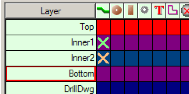
In addition to typing layer numbers, you can select View/Layer from the menu. You can also LMB click a layer in the Layer Display panel shown below:
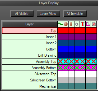

Lastly, you can use the Layer toolbar (shown above) to click among the active layers.
Changing layers is allowed while editing many objects. For instance, while you are routing you can change the layer to insert a via at the last corner.
Changing line width
The simplest way to change the width of a line while drawing is to press the ‘W’ key. This will invoke the Line Width Dialog. You can also RMB to get the context menu, which has a Change Line Width item.
Add a component to the board
If you want to manually add a component to your design (as opposed to automatically with a netlist) then the simplest way to do this is by clicking on the Add Component Button

or the Add Footprint Button on the Insert Object Toolbar. You can also choose Insert > Add Component or Insert > Add Footprint from the menu bar. Using the Add Component option allows you to choose from the library of parts that contains footprints that have been paired with symbols.
Using the Add Footprint option you can choose directly from the footprint libraries. Since these footprints have not been paired with symbols a generic symbol will be created when you place the part on your layout. You will find the schematic symbol for this footprint on the SyncPage_A.
Move a component
Depending on your experience, there may be a tendency to point at a component, hold down the LMB and drag that component. Though this is allowed, a much easier way is to point at the component and LMB click and release. This attaches the component to your cursor and allows you to do such things as use the RMB for context commands. You click once to select it and begin moving and click again to release it where you want.
Move a component to the other side of the board
Once you have a component selected the easiest way to move it from one side of the board to the other is by pressing the ‘O’ (for opposite) key on your keyboard. Alternatively, with the component selected you can RMB to display the context menu and select the Opposite command.
A component placed on the bottom of the board is automatically mirrored for you.
Rotate a component
Once you have a component selected on your cursor the easiest way to rotate it is to press the ‘R’ key on your keyboard. Alternatively, while you have the component on your cursor you can RMB to display the context menu and then select the Rotate command.
Component rotation is always performed counter-clockwise.
By default, component rotations are performed in 90-degree increments but you can change this default in the User Preferences - General dialog.
Edit a component
There are two ‘levels’ of component editing: you can edit information about the component and you can edit the contents of the component.
To edit information about the component and you have one or more components selected you can press Alt+Enter on your keyboard or alternatively RMB to display the context menu and select the Properties command to invoke the Component Properties dialog.
To edit the contents of a component, select a component, RMB to display the context dialog, and select the Edit Footprint command. This will invoke the Footprint Editor, which allows you to graphically modify the component contents such as pins and outline data.
Add a pin to the board
If you want to manually add a pin to your design, then the simplest way to do this is by clicking on the Add Pin Button

on the Insert Object Toolbar. You can also choose Insert/Pin from the menu bar.
Once you have selected this command, a default pin will be attached to your cursor and there will be a Pin Context Pane in the left panel that allows you to edit some of the more common pin properties.
Add a slot to the board
The PCB123 V5 Add Pin tool now includes a property to create slots on your layout and footprints. You can have up to 4 slots and cutouts on a layout when ordering through the PCB123 software. If you have more than 4 slots and cutouts you can go to wwww.sunstone.com and order through our Full Feature or Custom Quote service. Add a pin as described above and you will see the slot check box.
Select the Rectangle or Oval pad shape and set the pin properties for your plated or non-plated slots.
Move a pin
Only board-level pins can be moved in a design. To move component pins, you must edit the component in the Footprint Editor.
Depending on your experience, there may be a tendency to point at a pin, hold down the LMB and drag that pin. Though this is allowed a much easier way is to point at the pin and click it. This attaches the pin to your cursor and allows you to do such things as use the RMB for context commands. You click once to select it and begin moving and click again to release it where you want. Try it, it feels good.
Change a pin
If you have one or more pins selected you can press Alt+Enter on your keyboard or alternatively RMB to display the context menu and select the Properties command to invoke the Pin Properties Dialog which allows you to change any pin property.
Add a polygon or polyline
If you want to add a polyline or filled polygon to your design then the simplest way to do this is by clicking on the Add Polygon Button

on the Insert Object Toolbar. You can also choose Insert > Polygon from the menu bar.
Once you have selected this command, this symbol

will appear next to the cursor informing you that you are in Add Polygon mode and the system is waiting for you to click the first corner. After clicking the first corner, a line segment will then be drawn from the last corner clicked to the current cursor location. To stop digitizing the board outline you can either press the Esc key on your keyboard or just double-click the last corner.
If you double back over a line segment, the overlapping portion of the segment will be removed. You can keep doubling back to the previous corner to incrementally undo the board outline.
Once you have selected this command there will be a Polygon Context Pane in the left panel that allows you to edit some of the more common board outline properties.
You can also perform many of the global commands such as Change Grid while creating board outlines.
Add a circle
If you want to add a hollow circle to your design then the simplest way to do this is by clicking on the Add Circle Button

on the Insert Object Toolbar. You can also choose Insert/Circle from the menu bar.
Once you have selected this command, this symbol

will appear next to the cursor informing you that you are in Add Circle mode and the system is waiting for you to click the circle center. After clicking the circle center moving the mouse simply adjusts the circle radius. Click again at the desired radius to accept.
You can also perform many of the global commands such as Change Grid while creating circles.
Add an arc
If you want to add an arc to your design then the simplest way to do this is by clicking on the Add Arc Button

on the Insert Object Toolbar. You can also choose Insert/Arc from the menu bar.
Once you have selected this command, this symbol

will appear next to the cursor informing you that you are in Add Arc mode and the system is waiting for you to click one end of the arc segment. After clicking the arc start, you will be rubber banding a line. Click again to establish the arc end then any mouse movement will adjust the radius. After you have the desired radius click again to accept the arc.
You can also perform many of the global commands such as Change Grid while creating arcs.
Add a cutout
In V5 you can now add cutouts to your designs using the Create Cutout tool

. You can order through PCB123 with up to slots and cutouts in your layout. If you have more than 4 PCB123 will not allow you to order through the software. If you have more than 4 slots and cutouts you can go to the www.sunstone.com website to order through our Full Feature or Custom Quote service.

The cutout tool allows you to draw rectangular cutouts with up to 4 vertices and round cutouts. The cutout shapes are automatically included as part of your board outline. These objects can be moved and rotated independent of the board outline.
Move a board outline
To move an entire board outline just left click on it and drag, releasing the mouse button when you have position the board outline where you want.
Move board outline corners
Moving a board outline corner is simple: just point at a board outline corner, left-click, and release. Now you are moving a board outline corner. Just click again to release the corner where you want.
Delete board outline corners
Mouse over a board outline corner or corner or any polygon and press the d key. This process can also be accomplished with the mouse simply by selecting a corner and dropping it on the previous or next corner in the board outline. It is called corner reduction. It is very efficient, and can all be done with the mouse.
Insert corners in a board outline
To insert a corner in a board outline simply click on the middle third of a segment or at least .050” away from a corner. You will then be in digitizing mode that allows you to add corners until you stop by pressing the Esc key, double clicking, or inserting another corner at the same location as the previous one.
Add a connection between two pins
To add a connection between two pins click on the Connection Tool

to place the system in Add Connection Mode. Once in this mode simply click on the first pin you want to add the connection between. After clicking on the first pin, you will be rubber-banding a line while the system waits for you to click on the other pin that completes the connection.
If neither pin is tied to a net then a new, unique net name will be created for the connection. If one of the pins is tied to a net, then the connection and the other pin will inherit that net name. If both pins are tied to different nets then you will be prompted to merge the nets together.
Remove a pin from a net
To remove or disconnect a pin from a net first make sure you have the Select Object tool active then mouse over a pin you wish to disconnect. Right click on the pin and select Disconnect pin from net.
Alternatively, you can navigate to the pin in the Object Hierarchy tree and select Properties from the context menu. This will invoke the Pin Properties Dialog where you can either disconnect the pin from any net or assign it to a different net.
Start routing from a pin
If there is already a ratline (connection) tied to a pin simply click on it to begin routing. If the pin is a thru-hole pin then you will be routing on the current layer. If the pin is an SMD pin then the route will begin on whatever surface layer the pin is on. Once you have begun routing you can continue to digitize new corners until the route is completed or you press the Esc key to stop routing.
Alternatively, you can click on the FreeStyle Routing Tool

and then click on a pad to start routing. The same features as above apply in this mode with the only difference being if the pin was not previously tied to a net then a new, unique net name will be created with the pin and the route tied to it.
Start routing from another route
You can start a new route from a previous on by clicking on the FreeStyle Routing Tool

and then clicking on an existing route. The new route will inherit the net from the route you clicked on and you will be routing on the same layer as that route.
Add a via between layers
There are a few ways to add vias.
You can use the add pin tool to place a via manually at any location. This will create a via that is exposed through the solder mask and is thermally relieved when connected to filled polygons and plane layers.
A fanout via: To end a trace at a via you can start routing your trace at a pad. When you get to the location you would like to add your via left click and press the v key on your keyboard. A fanout via will be covered by solder mask and will be thermally relieved in a plane layer but not thermally relieved in a filled polygon.
Add a via while routing a trace and continue routing on another layer: Start a trace at a pad and route to the location you will need a via. Left click to stop the trace. If you are routing on a two layer board you can press the z key on your keyboard. This will add a via and switch you to the opposing layer to continue routing. If you are routing on a multi-layer board you can use the number key across the top of you keyboard to add a via and switch layers to continue routing. This type of via will be covered by solder mask and will be thermally relieved in a plane layer but not thermally relieved in a filled polygon.
1 = top
2 = bottom
3 = inner layer 1
4 = inner layer 2
5 = inner layer 3
6 = inner layer 4
Example:
You are routing on the top layer and you want to add a via and continue routing on layer 2 (inner layer 1) of a multi-layer board: Start your trace from a pad on the top layer. Route to the location you will need a via. Left click and press the number 3 key across the top of your keyboard. This will add the via and switch to inner layer 1 (layer 2 of your layout) to allow you to continue routing. Route the trace to the desired end-point.
An alternative to using the number key across the top of your keyboard is to use the toolbar on the far right side of your screen. This toolbar works just like pressing the number keys across the top of your keyboard. Press the button corresponding to the layer you would like to continue routing on. A description of the buttons follows.
Insert corners in a route
To insert a corner in a route simply click on the middle third of a segment, or at least .050” away from a corner and you will by in a digitizing mode that allows you to add corners until you stop by either pressing the Esc key or double clicking to auto-complete the segment. It is easy to tell if you are in Insert Corners mode because the segment you click on is essentially “ripped up” and will show a ratline from the cursor to the next corner.
Delete route corners
Mouse over a corner and press the d key to delete a corner. This process can also be accomplished with the mouse simply by selecting a corner and dropping it on the previous or next corner in the board outline. It’s called corner reduction. It is very efficient and can all be done with the mouse.
It can also be accomplished by getting into Insert Corners mode and effectively routing “backwards” as doubling back over existing corners has the effect of removing them.
Move a route corner
Moving a route corner is simple: just point at a corner, left-click, and release. Now you are moving the corner. Just click again to release the corner where you want.
Releasing the corner over the prior or next corner has the effect of deleting the prior or next segment.
Move a route segment
If you point at a route segment and hold down the left mouse button while dragging, the entire route segment will move with the cursor.
Change the width of a route segment
You can only change the width of an individual route segment while you are routing by pressing the ‘W’ key on your keyboard or RMB and selecting Width… from the context menu. To change the width of an existing route segment you must first click on that segment to get into Insert Corner mode and then press the ‘W’ key.
Add text to the board
If you want to add text to your design then the simplest way to do this is by clicking on the Add Text Button

on the Insert Object Toolbar. You can also choose Insert/Text from the menu bar.
Once you have selected this command you will immediately be prompted for the string to add with the Add Text Dialog. After entering a string and dismissing the dialog a piece of text will be attached to your cursor. While it is attached you can press the ‘R’ key to rotate it, the ‘W’ key to change its width, or a layer number to change its layer. When changing its layer interactively it will automatically toggle its mirrored state between the top and bottom layer.
Whenever you have a piece of text attached to your cursor you can modify many of its properties then and there in the Text Pane of the Edit Panel. You can always select Properties on the text to display the Text Properties Dialog.
You can also perform many of the global commands such as Change Grid while creating text.
Rename a component
If you are new to PCB123 renaming a component may appear counter-intuitive at first because you may just point at a reference designator text object and attempt to change its name only to find that you can’t. You must select the component object and change its name in the Component Properties Dialog. The text object is just a manifestation of a macro placeholder (&RefDes) that inherits its value from the component reference designator. When you change the component name the text will automatically reflect the new name.
When you rename a component for the first time a special attribute record is generated internally that remembers the original name. The original name will appear in a BOM Report so you can back-annotate your schematic if you so desire. This is also to facilitate the automatic back-annotation of schematics in the future.
Pan
You have two options to pan the display. Both options work in both layout and schematic.
Option 1: Hold down shift and move your mouse.
Option 2: Hold down the right mouse button and move your mouse. This option is new to version 5.1 and has some optimized display options to make panning very smooth.
Designing a board without a netlist
Depending upon the nature or complexity of the design, you may opt to skip a schematic altogether and start right in on the physical layout. In this case, you probably will not use or need a netlist or a schematic editor. PCB123 can support you on these very simple designs as well. Just dive right in with physical layout.
About loading a Netlist
If you have captured your design in a schematic tool then you should be able to create a netlist that PCB123 can import. If you use the PCB123 schematics package to capture your design then any device you use from the standard libraries will be mapped to a footprint in the layout software.
If you are using a third party schematics package it should be able to emit a Tango or Protel formatted netlist that can be read into the PCB123 layout software. The devices you use in the third-party schematics package most likely will not specify an explicit footprint that matches the PCB123 library. Not to fear: when you load a netlist that specifies footprints that cannot be matched in the library, or a netlist that only specifies part types then during the netlist load process you will be prompted to browse for a footprint with a very flexible tool called the Part Browser. This tools lets you perform a search against various criteria and graphically preview the footprints. Once you have selected a footprint to use you will be given the opportunity to let the system forever remember the mapping between your part type and the footprint you chose for that part. It will not ask for a footprint again when it encounters that part.
You can import your netlist from three different locations.
The new board wizard.
The board configuration on the first run.
With a board in view select Design > Netlist > Compare/Update Design. This is just about the same as previous version. After you have selected the netlist you will see the new UI shown below.
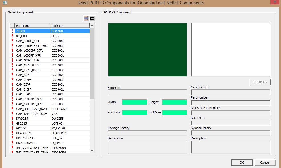
The red ! in the left column tells you that you have not selected a footprint for this row. The second column is the name of the symbol in your netlist. The third column is the name of the footprint from your netlist. Select a row and then go up to the two buttons in the upper right corner of the table  . The left button
  allows you to select a part from the parts taxonomy. The right button
  allows you to select a part directly from the footprint libraries.
As you select your parts you will see the red ! change to green check marks. Once you have all of the parts selected you can select the OK button and all of the parts will be placed on a blank board outline.
If you encounter an error you may have selected a footprint that does not match the information listed in your netlist. You will see a popup text dialogue with information that will help you to locate the issue. After selecting the correct footprint select OK and you will arrive at your layout with all of the parts on the screen.
Go directly to Design > Netlist > Compare/Update Design to make your modifications.
Starting the layout with a netlist opens a large array of benefits that you may or may not take advantage of. They include:
Autoplace – You can run the Autoplace tool. This tool can be real handy just to gauge board density and get a feel for the overall flow of routing.
Placement Optimization – You can easily see what is connected to what as you place components on the board. In addition, the length of nets is continuously optimized as you move part around.
Easier Rules Specification – With all nets specified at once you can specify which ones need special width or spacing considerations and establish which nets are tied to any plane layers.
Fanout and Autorouting – With a complete netlist loaded, you can run automatic tools that fanout surface mount devices and autoroute your board. Even if you don’t normally use an autorouter running it can identify trouble spots in your design.
Automatic ECO – If you make a change to your schematic after your layout has been started you can compare the new netlist against the design and have the system automatically make the necessary changes to the design so that it matches the new netlist.
